Growing of heteroepitaxial layers on lattice mismatched substrates by the method of scanning liquid phase epitaxy
Abstract
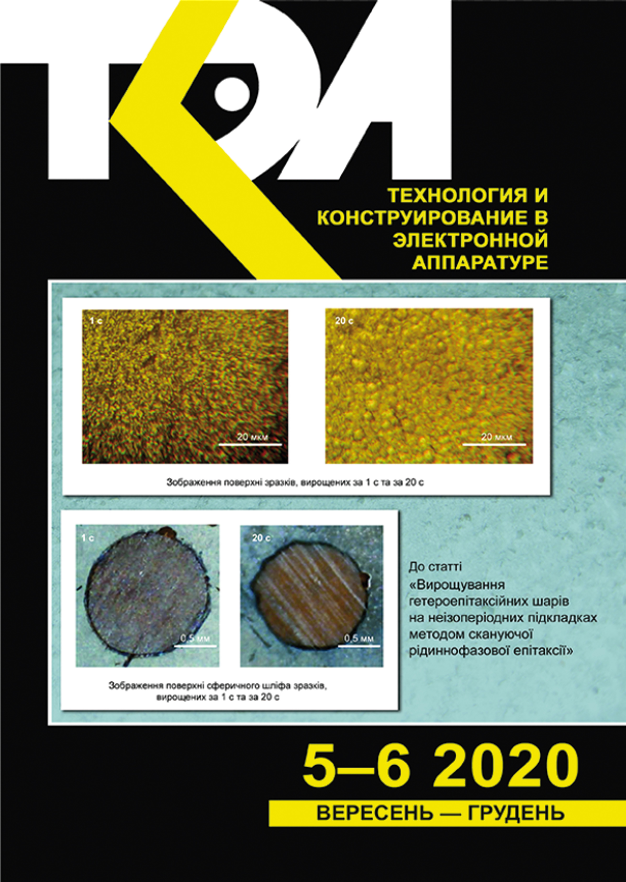
Heterostructures with lattice mismatched and compositionally different layers are widely used in modern electronic and optoelectronic device engineering. Generally such structures are manufactured by the methods of metal-organic vapor phase epitaxy, metal-organic chemical vapor deposition and molecular-beam epitaxy. However, the methods of deposition from a liquid phase are the most inexpensive and simple yet. Thus obtaining the above mentioned heterostructures from a liquid phase is still promising. In this work we demonstrated the possibility of using the method of scanning liquid phase epitaxy to grow continuous heteroepitaxial layers over the substrate surface highly mismatched by lattice constant and having different crystal-chemical properties. By controlling basic parameters of the method we created the conditions close to the solution-melt saturation limit. In other words, we created the conditions of ultra-fast solution-melt cooling and, respectively, high growth rate. We obtained the heterostructures of Ge layers grown on GaP substrates where the lattice mismatch made 3.7%. Gallium was used as the solvent for Germanium. The heterostructure was grown by the method of scanning liquid phase epitaxy in the conditions of ultra-fast initial cooling of the solution-melt. Overcooling at the crystallization front was controlled by an extra heater of the substrate back side. The growing time was 1 and 20 seconds for the two test samples. The layers thickness was determined by the spherical slice technique to be 1.2 and 1.5 μm for these two growing time values, accordingly. We showed that it was possible to obtain more perfect Ge layers on GaP substrate by lowering the growth rate in the final growth stage.
This method can be used to grow heterostructures used in creating such modern electronic and optoelectronic devices as structures based on A3B5 compounds and their solid solutions, which cannot be obtained by other classical methods of liquid phase epitaxy due to significant differences in lattice constants and / or crystal-chemical properties.
References
Li Q., May Lau K. Epitaxial growth of highly mismatched III-V materials on (001) silicon for electronics and optoelectronics. Progress in Crystal Growth and Characterization of Materials, 2017, vol. 63, pp. 105-120. https://doi.org/10.1016/j.pcrysgrow.2017.10.001
Zhao C., Xu B., Wang Z., Wang Z. Boron-doped III-V semiconductors for Si-based optoelectronic devices. Journal of Semiconductors, 2020, vol. 41, iss. 1, 011301. https://doi.org/10.1088/1674-4926/41/1/011301
Mishra P., Nguyan A., Chen P.W., Tseng C.K., Lee M.C. Implementation of lateral Ge-on-Si heterojunction photodetectors via rapid melt growth and self-aligned microbonding for Si photonics. Japanese Journal of Applied Physics, 2019, vol. 58, SJJC02. https://doi.org/10.7567/1347-4065/ab24b3
Viheriala J., Aho A., Isoaho R., Aho A., Tukiainen A., Guina M. Quantum-well laser diodes operating at 1.28 μm monolithically integrated on Ge substrate. Proceedings 10537. Silicon Photonics XIII. 105370U (2018). https://doi.org/10.1117/12.2292738
Lan D., Green M. Up-conversion of sunlight by GaInP/GaAs/Ge cell stacks: Limiting efficiency, practical limitation and comparison with tandem cells. Energy Procedia, 2017, vol. 130, pp. 60-65. https://doi.org/10.1016/j.egypro.2017.09.396
Tournet J., Parola S., Vauthelin A. et al. GaSb-based solar cells for multi-junction integration on Si substrates. Solar Energy Materials and Solar Cells, 2019, vol. 191, pp. 444-450. https://doi.org/10.1016/j.solmat.2018.11.035
Baidus N.V., Aleshkin V.Y., Dubinov A.A. et al. On the Application of Strain-Compensating GaAsP Layers for the Growth of InGaAs/GaAs Quantum-Well Laser Heterostructures Emitting at Wavelengths above 1100 nm on Artificial Ge/Si Substrates. Semiconductors, 2018, vol. 52, pp. 1547-1550. https://doi.org/10.1134/S1063782618120060
Bolkhovityanov Yu.B., Pchelyakov O.P., Socolov L.V., Chikichev S.I. Artificial GeSi substrates for heteroepitaxy: Achievement and problems. Semiconductors, 2003, vol. 37, no. 5, pp. 493-518. https://doi.org/10.1134/1.1575352
Roychowdhury R., Dixit V.K., Vashisht G. et al. Surface and interface properties of ZrO2/GaAs, SiO2/GaAs and GaP/GaAs hetero structures investigated by surface photovoltage spectroscopy. Applied Surface Science, 2019, vol. 476, pp. 615-622. https://doi.org/10.1016/j.apsusc.2019.01.103
Oshima R., France R., Geisz J. et al. Growth of lattice-matched GaInAsP grown on vicinal GaAs(001) substrates within the miscibility gap for solar cells. J. Cryst. Growth, 2017, vol. 458, pp. 1-7. https://doi.org/10.1016/j.jcrysgro.2016.10.025
Barrutia L., Garcia I., Barrigjn E. et al. Impact of the III-V/Ge nucleation routine on the performance of high efficiency multijunction solar cells. Solar Energy Materials and Solar Cells, 2020, vol. 207, 110355. https://doi.org/10.1016/j.solmat.2019.110355
Li X., Zhao Y., Wu Q. et al. Exploring the optimum growth conditions for InAs/GaSb and GaAs/GaSb superlattices on InAs substrates by metalorganic chemical vapor deposition. J. Cryst. Growth, 2018, vol. 502, pp. 71-75. https://doi.org/10.1016/j.jcrysgro.2018.09.003
Ghosh S., Rodrigues L., Moura L., Ferreira S. Epitaxial growth and characterization of Cd1-xMnxTe films on Si (111) substrates. J. Cryst. Growth, 2019, vol. 522, pp. 25-29. https://doi.org/10.1016/j.jcrysgro.2019.06.009
Desplanque L., Bucamp A., Troadec D. et al. Selective area molecular beam epitaxy of InSb nanostructures on mismatched substrates. J. Cryst. Growth, 2019, vol. 512, pp. 6-10. https://doi.org/10.1016/j.jcrysgro.2019.02.012
Nakasu T., Sun W., Kobayashi M., Asahi T. Effect of Zn and Te beam intensity upon the film quality of ZnTe layers on severely lattice mismatched sapphire substrates by molecular beam epitaxy. J. Cryst. Growth, 2017, vol. 468, pp. 635-637. https://doi.org/10.1016/j.jcrysgro.2016.11.035
Rao Y., Zhang H., Yang Q. et al. Liquid phase epitaxy magnetic garnet films and their applications. Chin. Phys. B, 2018, vol. 27. iss. 8, 086701. https://doi.org/10.1088/1674-1056/27/8/086701
Tsybrii Z., Bezsmolnyy Yu., Svezhentsova K. et al. HgCdTe/CdZnTe LPE epitaxial layers: From material growth to applications in devices. J. Cryst. Growth, 2020, vol. 529, p. 125295. https://doi.org/10.1016/j.jcrysgro.2019.125295
Donchev V., Milanova M., Georgiev S. et al. Dilute nitride InGaAsN and GaAsSbN layers grown by liquid-phase epitaxy for photovoltaic applications. J. Phys.: Conf. Series, 2020, vol. 1492, p. 012049. https://doi.org/10.1088/1742-6596/1492/1/012049
Ci J.-W., Lian C.-Y., Uen W.-Y. et al. Formation mechanism of high Ge content SiGe epilayer on Si by liquid phase epitaxy using Ge-Sn solution. Thin Solid Films, 2020, vol. 704, p. 137981. https://doi.org/10.1016/j.tsf.2020.137981
Long J., Xiao M., Huang X. et al. High efficiency thin film GaInP/GaAs/InGaAs inverted metamorphic (IMM) solar cells based on electroplating process. J. Cryst. Growth, 2019, vol. 513, pp. 38-42. https://doi.org/10.1016/j.jcrysgro.2019.02.057
Reisinger M., Ostermaier C., Tomberger M. et al. Matching in-situ and ex-situ recorded stress gradients in an AlxGa1-xN heterostructure: Complementary wafer curvature analyses in time and space. Scripta Materialia, 2018, vol. 147, pp. 50-54. https://doi.org/10.1016/j.scriptamat.2017.12.016
Abramov A.V., Deryagin N.G., Tret'yakov D.N. Application of superfast (102-103°C/s) cooling of a solution-melt in the liquid-phase epitaxy of semiconductors. Semiconductors, 1999. vol. 33, no. 9, pp. 1130-1133.
Tsybulenko V.V., Shutov S.V., Yerochin S.Yu. LPE application technique for obtaining of thin film semiconductor materials. Proc. 1st Intern. Electronic Conf. on Crystals (IECC 2018). 2018. https://doi.org/10.3390/IECC_2018-05250
Tsybulenko V., Shutov S., S. Yerochin Determination of crystallization conditions of Ge/GaAs heterostructures in scanning LPE method. Semiconductor Physics, Quantum Electronics & Optoelectronics, 2020, vol. 23, no 3, pp. 294-301. https://doi.org/10.15407/spqeo23.03.294
Tsybulenko V., Shutov S., Boskin O. The features of scanning liquid phase epitaxy technique as applied to thick epitaxial layers growth. KPI Science News, 2020, no 3, pp. 58-64. https://doi.org/10.20535/kpi-sn.2020.3.197877 (Ukr)]
Sokolov I.A. Raschety protsessov poluprovodnikovoy tekhnologii [Calculations of Semiconductor Technology Processes]. Moscow, Metallurgiya, 1994. (Rus)
Chernov A.A. Modern Crystallography III: Crystal Growth. Springer Science & Business Media, 2012. https://doi.org/10.1007/978-3-642-81838-7
Lyakyshev N.P. Diagrammy sostoyaniya dvoynykh metallicheskikh sistem. T. 2. [State Diagrams of Double Metal Systems. Vol. 2]. Moscow, Mashinostroenie, 2000. (Rus)
Copyright (c) 2020 Tsybulenko V. V., Shutov S. V.

This work is licensed under a Creative Commons Attribution 4.0 International License.
